Printed Circuit Board layout projects for third-party Customers
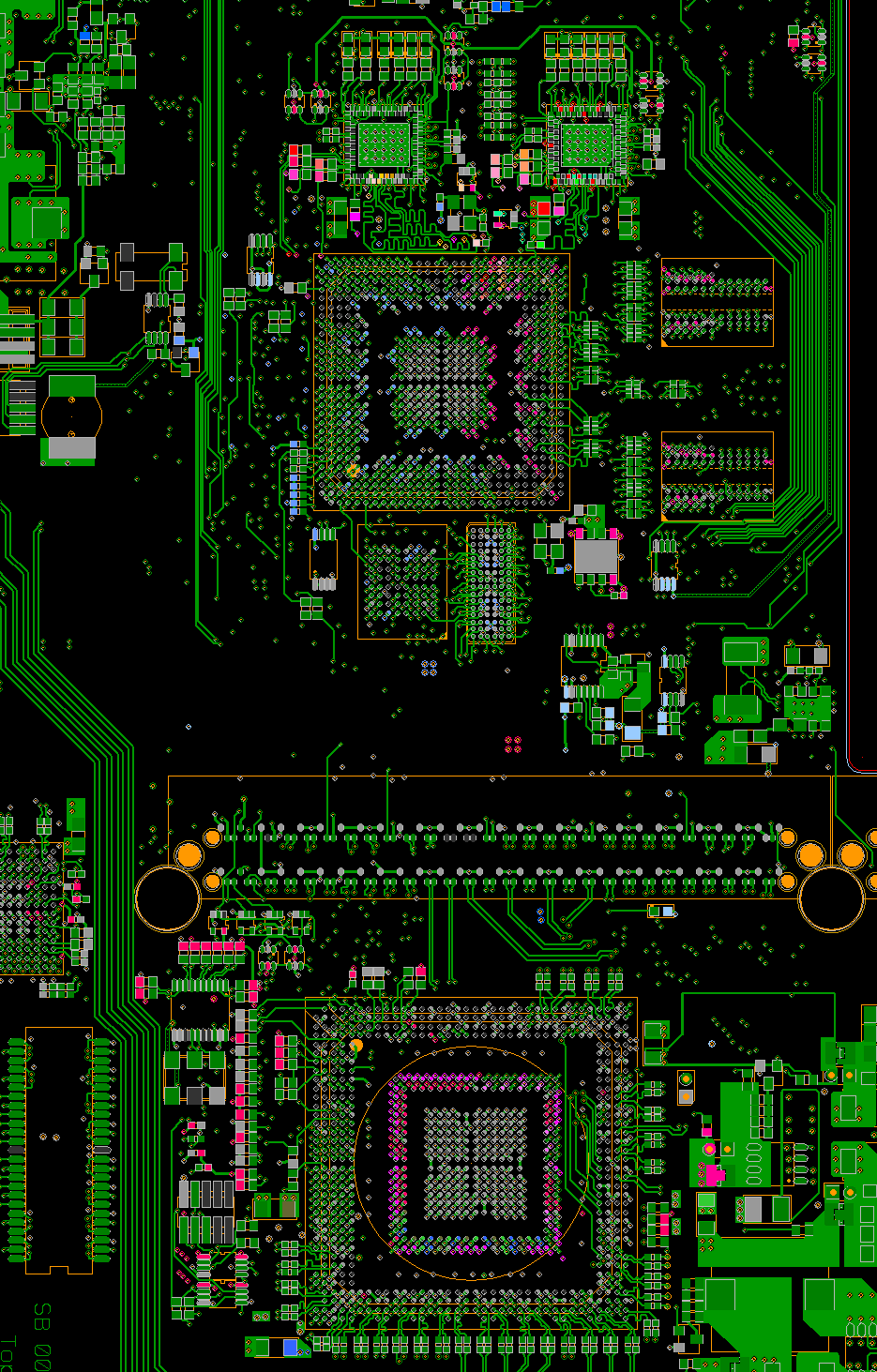
PCB Layout Design ATCA ADSL board project
Features:
- Board Size: 282 X 322.25 (mm)
- Pins: 24011
- Layers: 10
- Nets: 5205
- Connections: 17303
- Parts: 5657
- Design time: two month (8 weeks)
PCB Layout Design ATCA Base & Fabric HUB project
Features:
- Board Size: 282 X 322.25 (mm)
- Pins: 16181
- Layers: 10
- Nets: 3326
- Connections: 11798
- Differential Pairs: 474
- Parts: 3862
- Design time: two month (8 weeks)
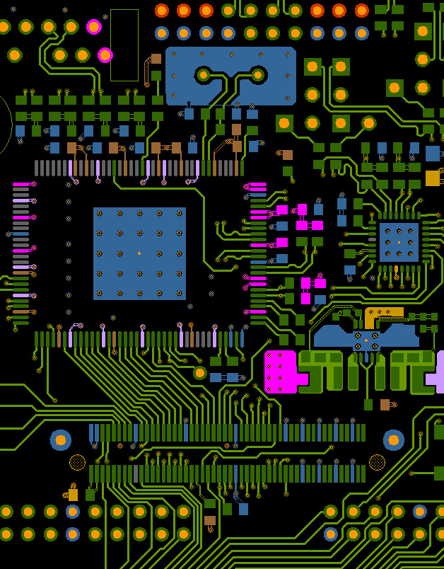
PCB Layout Design Artix_STM Evolution development board project
Features:
- Board Size: 137 X 137 (mm)
- Pins: 1853
- Layers: 4
- Nets: 456
- Connections: 1336
- Differential Pairs: 32
- Parts: 615
- Design time: two weeks
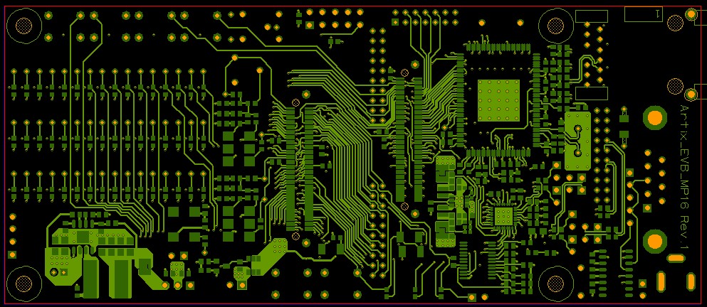
PCB Layout Design Artix_TDM Evolution development board project
Features:
- Board Size: 60 X 140 (mm)
- Pins: 1355
- Layers: 4
- Nets: 361
- Connections: 947
- Differential Pairs: 16
- Parts: 426
- Design time: 8 working days


