A successful PCB layout project depends on the design of the stack (layer structure)
Proper stackup design is important because it forms the basis of a successful printed circuit board (PCB) design.
Newer ICs today have edge rates in the sub-nanosecond range; the fastest of which are multi-gigabit transceivers that have edge rates of less than 100ps. With such fast edge rates, it is important to tightly control trace impedance to meet signal integrity requirements and have consistent reference planes to meet our electromagnetic compatibility requirements.
It is also essential that we explore stackup options so as not to compromise board yields as well as add unnecessary cost to the manufacturing process.
When developing a stack it is important to work out different versions of its layout. It takes into account the possibility of production. the complexity of the manufacture of this structure layers and the avoidance of additional costs in the manufacture of printed circuit boards.
Design and optimization of the structure of layers (stackup) of the PCB

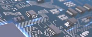
Pic 1. Stackup example
There are four key things to be considered when designing a good stackup for a printed circuit board. They are:
- Signal Integrity
- Crosstalk
- Electromagnetic Interference
- Manufacturing Costs
Signal Integrity
Signal Integrity is a measure of signal quality. In a digital system, a signal with ideal signal integrity resembles a trapezoid.
In reality, there is always some distortion of the signal on the board. There is always the question of how much the board distorts the signal and how this affects the functionality and reliability of the product. Distortion of the waveform can be so severe that it will affect the time intervals and lead to the inoperative state of the product as a whole.

Pic 2. Eye diagram
Ringback, overshoot, undershoot and non-monotonic edges are some of the metrics used to measure signal quality in digital PCB design.
The two primary factors that affect signal integrity of highspeed signals on a PCB are impedance discontinuities and loss (resistive and dielectric).
Impedance Discontinuities
Different signaling technologies require different traces impedances. As an example, the recommended traces impedances for DDR and DDRII are 60 ohms and 50 ohms respectively. The instantaneous impedance of a trace on a PCB is determined primarily by the trace width and dielectric thickness.
To attain the desired trace impedances for our designs, we need to determine the required trace and stackup parameters. This data can usually be provided by the board fabrication house based on the type of material they have in stock and their fabrication process.
Crosstalk
The coupling of energy (mutual inductance and capacitance) from one PCB trace to another is crosstalk. A good stackup design can significantly reduce the amount of crosstalk that is seen on a PCB. In digital designs inductive crosstalk usually dominates capacitive crosstalk.

Pic 3. Crosstalk
Inductive coupling results from return currents which generate magnetic fields in other traces leading to crosstalk.
There are three primary methods of reducing crosstalk on a PCB. The easiest, yet most costly of these, is having adequate spacing between adjacent traces so that crosstalk is never a concern. A common figure of merit that is used is 3X the dielectric height. For example, if you have a 5 mil dielectric height, you would need to have a minimum of 15 mils between traces on the layer. This is an impractical approach for most of today’s high density boards. It would require extra layers or a larger board design to meet this requirement.
The other two approaches to controlling crosstalk, routing on striplines as opposed to microstrips and reducing dielectric height, are more feasible and have less impact on the cost of the design.
Electromagnetic Interference (EMI)
Radiation of energy from one electronic device to another capable of disrupting the proper functioning of the latter is Electromagnetic Interference.
Compliance to EMI standards, such FCC, CISPR or VCCI are influenced by signal integrity and crosstalk performance of a given PCB. Controlling signal integrity and crosstalk reduces the EMI on a PCB.

Pic 4. Electromagnetic Interference (EMI)
In designing a PCB, a lot of effort usually goes into designing the path of the signal. We often do not consider the return path of the signal.
Since current flows in a closed loop, every signal has a loop areas associated with it. There are several sources of EMI on a PCB. A significant one is the loop area around which a high-speed signal propagates.
As a result, in designing a stackup, a guideline to reduce EMI is to reduce the current loop area. This could be the loop area from reference plane gaps as well as loop area created between a signal and its reference plane.
Manufacturing Costs
The cost of manufacturing a PCB can contribute to the success of the product.
Any manufacturing cost is always passed onto the consumer, so it is important to ensure that a product has the lowest price-point possible to stay competitive.
It is important for designers to work hand-in-hand with PCB material vendors and fabrication facilities to determine what type of materials are available to meet the design needs at the lowest costs. Whenever possible, it’s always best to choose materials that are available in-house to avoid special order items and minimize the cost of the design.
This includes choosing dielectric heights for the design based on the laminate thicknesses that are available to the board house you will be working with. Any material outside the list of commonly used products will result in increased board cost.
Summary
A successful PCB design depends heavily on the stackup design. A good stackup can enable designers optimize their designs for signal integrity, crosstalk and EMI.
For signal integrity, it is important for designers to minimize discontinuities in their topologies.
They can reduce crosstalk on their PCBs if they tightly couple (where possible) signal to reference planes. They can also reduce EMI by increasing coupling to their reference planes as well as (where possible) shielding signal by routing them partially or completely as striplines.
Reducing dielectric thickness
Reducing the electromagnetic effect (radiation) is also achieved by reducing the thickness of the dielectrics as well as shielding the conductor with their partial or full transfer to the inner layers. Careful selection of materials for a stack also reduces the cost of manufacturing a printed circuit board.