Types of PCB and description of the design process
The printed circuit board is a dielectric plate, where conductive circuit of an electronic circuit is formed on the surface by a volumetric form. Printed circuit board is used by electrical and mechanical way to connect and diversified electronic components.
Outputs in electronic components joined by conductive pattern elements soldering.
The electrically conductive pattern is made by foil on solid insulating. There must be holes for mounting and contact pads what enables mounting SMD or through-hole components in each circuit board.
If the plate has multiple layers, it must have vias for electrically connecting portions of the foil, which is located on different layers of the board.
There is “solder mask”, which is a protective coating on the external side of the board. Also every board is required to be marked, so it must have text and auxiliary picture that is performed according to the design documentation.

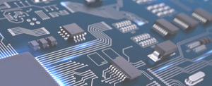
Pic 1. Appearance of PCB board
Types of printed circuit board
Printed circuit boards can be divided into 3 groups:
- Single sided PCB.The conductive pattern is on the one side of the insulating base. There are non-metallized through holes that occurs mechanical fixation. All printed conductors end pads, which are used for the connection. If there is a conflict of intersecting routes, it can be resolved by installing a curtain wire jumpers.
- Double sided board. That’s a lot of thin insulating substrates to be coated conductive pattern, and then they are physically connected to one multi-layer substrate. Electrical connections are made via the through or blind holes. Each layer has its own function in the multi-layer boards.
- Multilayer printed circuit boards. That’s a lot of thin insulating substrates to be coated conductive pattern, and then they are physically connected to one multi-layer substrate.
Electrical connections are made via the through or blind holes.
Each layer has its own function in the multi-layer boards:
- The outer layers are used for mounting electronic components.
- Signal layers are used for signal interconnection topology map.
- Some layers are heat-align.
- There is a power and ground layers. They have large polygons with minimal inductance and ohmic resistance.
These layers are used as electric screens, buyout grounded for high frequency decoupling capacitance:
- The outer layers are used for mounting electronic components
- Signal layers are used for signal interconnection topology map
- Some layers are used for heat sink and heat distribution
- There is a power and ground planes layers. They have large polygons with minimal inductance and ohmic resistance. These layers are used as electric screens, and are grounded for high frequency decoupling capacitance.

Ріс 2. Printed circuit board with vias
There is another classification of PCBs:
- Flexible printed circuit boards. They have a thin and flexible substrate. They are used to connect the various parts of electronic devices that run on a rigid base. Flexible boards are used as a base for the antenna, inductors, etc.
- Flex-rigid printed circuit boards. They are both flexible and rigid boards simultaneously. They are very difficult to be made.
- Board with non-through vias. These boards are made with using technologies of laser microvia, drilled “blind” and “buried” vias.
- Metal Core PCB. Are used when it is necessary to dissipate more heat output. They often used for powerful SMD LEDs boards.
- Printed circuit boards for high frequency applications. Used for high-frequency devices. To manufacture such kind of boards are used Teflon, PTFE and other materials.
- PCBs for LED solutions. Used for powerful LEDs technology.
- HDI PCBs (High Density Interconnect). Boards have a very high density of interconnections.
Development stages of PCB designing
PCB design is a long process and it consists of several stages. It is necessary to take into account the IPC standards, the requirements for the production and testing, operating mode, thermal analyze.
Schematic and requirements
To start with board design designer have to receive from customer next project data:
- Circuit schematics and principal operation diagram.
- List of components containing links to the manufacturing documents (datasheets). Board drawings specifying dimensions, configuration, mounting holes, connectors and button locations, LED mount height, areas without traces, areas without components, areas with limited mount height etc.
- Information specifying board constraints: the number of layers, circuit groups parameters (differential pairs, clock signals, high-voltage circuits, power circuits etc.), components with high power dissipation etc.
Components Library
The next step is components library creation. Footprints must be created according JEDEC or IPC standards or datasheet information.
Components placement
Than designer makes preliminary global components placement on the board. Discuss it with customer. The components are placed according to the requirements. Some components have fixed positions according customer requirements or board form-factor specifications. 3D model of board with components can be created on this designing stage. Customer can check product case with PCBs 3D model for possible mechanical discrepancy. Final components placement. Components placement optimization.
Trace routing
At this stage designer define and setup physical trace parameters such as width, trace spaces etc. Also board stack up is created according project complexity and manufacture capabilities. Trace routing can be implemented by hand (manual) routing or by automatic routers.

Pic 3. PCB Trace routing
Signal simulation
After board trace routing is completed designer have to make trace simulation to find out possible signal degradation and product operation failure. To avoid routing mistakes board is checked with signal and power integrity simulation, electromagnetic protection analyze and thermal dispersion modelling.
Board checking and final data output
At final stage the completed design is checked with DRC (Design Rule Checking). Manufacturing Data is generated from full completed and verified design. Data for manufacture consists of Gerbers, ODB++ files, assembly and FAB drawings, components coordinates report for automatic assembler etc.
All these data is transferred to customer.